Project Area
Biomedical Instrumentation
Undergraduate Research
A mixed-signal hardware platform developed to acquire the small sensor signals used in ballistocardiography research, with an emphasis on PCB design, reliable hardware bring-up, measurement, troubleshooting, and scalable deployment.
Project Area
Biomedical Instrumentation
Hardware
Mixed-Signal PCB
My Role
Undergraduate Research Assistant
Focus
Design, Bring-Up, and Validation
What Is BCG?
A ballistocardiogram, abbreviated BCG, records the subtle motion of the body associated with cardiac contraction and the ejection and movement of blood. Unlike an electrocardiogram, which measures the heart’s electrical activity, ballistocardiography focuses on a mechanical response.
These motions are small, so the acquisition electronics must handle low-level sensor signals while preserving useful physiological information. That requirement makes board layout, grounding, power, component selection, signal integrity, and repeatable validation central engineering concerns.
This project focused on the data-acquisition hardware used in a university research platform. The PCB work supports signal capture and experimentation; it is not presented here as a medical device or diagnostic product.
My Contribution
As an undergraduate research assistant at Texas State University, I helped relaunch and improve a faculty-developed ballistocardiogram data-acquisition platform. My work covered the complete board-level engineering loop rather than ending when the PCB layout was complete.
Development Workflow
Review the research platform’s sensing, acquisition, interface, power, and mechanical needs before beginning the board design.
Develop the schematic and physical layout while separating sensitive mixed-signal paths and accommodating the required connectors and devices.
Assemble and inspect the board, verify power and reference points, and test interfaces in a controlled sequence.
Use laboratory instruments to evaluate behavior, isolate faults, validate revisions, and feed findings back into the next design iteration.
Hardware Development
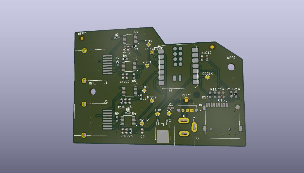
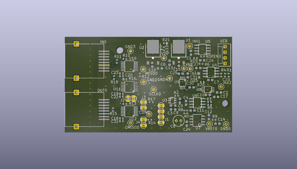
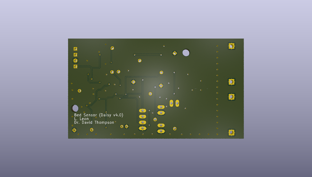
The available board designs show the evolution of the acquisition electronics, component placement, connectors, test points, and mechanical outline. Three-dimensional PCB renders were used to review layout and integration before fabrication and assembly. KiCad was used for schematic capture, PCB layout, and three-dimensional board review throughout the design process.
Bring-Up and Validation
Hardware bring-up used staged checks so that power, references, interfaces, and signal paths could be evaluated before complete system operation. A Digilent Analog Discovery 3 provided oscilloscope and logic-analyzer measurements, giving direct evidence of circuit behavior and helping isolate board-level faults.
The results informed subsequent revisions and practical improvements to component availability, cost, manufacturability, and deployment. This work connected schematic and layout decisions with measured performance on physical hardware.
I also created the project bill of materials to organize component and sourcing information. To help the research continue beyond my involvement, I shared the accumulated design information, test data, and troubleshooting knowledge with the next group of research students.
Continue Exploring